The P7 was the first prototype for an op-amp to use a varactor diode bridge as a means of producing an error signal amplified by transistors (rather than the conventional vacuum tubes or the later FETs). Conceptualized by George A. Philbrick (or Lewis R. Smith?), the prototype was simplified (well, a nitpicker may argue the extra circuit current) by Bob Malter resulting in one of the most profitable operational amplifiers ever to be sold, the P2.
Sporting input bias currents in the pA range (1x10e-12), the P2 drove a $220 demand, which was 1/8 to ½ (my source for this one is obscure) the price of a VW Beetle at the time. The cost of building a P2 paralleled that of a cheap radio – around $10 to $15, so you can just imagine how lucrative things were. The P2 dominated for 30 years, becoming obsolete only after the release of the LMC660, which now offers input bias currents at the fA range (1x10e-15).
My interest for the P2 was piqued once more by Paul Rako’s great post “What’s All this Varactor Input Amplifier Stuff, Anyhow?”. In the article, he delved into an improved schematic from the late Bob Pease and attempted a computer simulation out of it, an endeavor that proved partially unsuccessful due to unaccounted parasitics and magnetics.
Anyway, we found out from the comments that LTSpice had the older form of the circuit, the P2, as an educational example. I am embarrassed myself of not knowing it was there and fortunate to discover that it was. So, here was a circuit, a high-profile industrial secret 40 years ago, free to the public for tweaking and vandalizing. It is an opportunity to expand our horizons on operational amplifier function and design, so I had a go at a couple of simulations below. Hopefully, I don’t hear Mr. Philbrick’s voice shouting at me anytime soon.

Figure 1. Schematic of the P2 in LTSpice.
The op-amp is configured as a simple inverting amplifier. The source is a pulse generator at 200mVpk-pk [0V DC offset] with an on and off time of 0.5 ms. Rise and fall times are set to 0.1 ms (why? Bob Pease mentioned in Jim William’s book that the slew rate of the P2 was awful – 0.03V/µsec. The P2 needed 33.33 µs to reach 1V at the output. Yuck! We’ll see the tolerance range for the rise and fall times in Part 2, where the circuit is truly vandalized). All current is flowing at R35 and the feedback resistor R3. 10µA will induce a 1V drop at R3. Since the other terminal is referenced to ground, the output voltage during the positive cycle of the input will be an inverted 1V [and vice versa during the negative cycle].
The alternative textbook formula [which I’ve grown to hate] for the gain of an inverting op-amp is -Rf/Ri. Such shortcuts have become lethargic to me. Solving yields –(100kohm/10kohm) = -10.
You yourself may try the simulation out, and due to excitement, get an immediate figure similar to the one below.

Figure 2 Immediate simulation result of the P2 in LTSpice.
The input is, of course, at the end of the resistor pulled down to ground by the coils of the bridge. You won’t get that from an ideal op-amp [re-drawn below for convenience].

Figure 3 Inverting amplifier configuration using an ideal op-amp.

Figure 4 Simulation result for the schematic in Figure 3.
For comparison, below is the simulation result of the P2 with the probe on the input pulse.

The strange trend at the output between 0 ms to 0.1 ms is because the output hasn’t reached 1V yet, so I introduced a delay of 0.1ms, to ensure that the cause isn’t effectuated by the start-up of the circuit.

Figure 5 Simulation result of the P2 with a delayed pulse.
Now to figure out the functions of each branch in the circuit. If my assumptions are correct, the labelled figure below should suffice to properly identify each region.

Figure 6 Comprehensive block analysis of the P2.
The oscillator feeds a sinusoidal “carrier” to the diode bridge to modulate the inputs. DC isolation is provided by the transformers. In reality, 2 pairs of well-matched diodes offset the leakage currents to a minimum.

Figure 7 Simulation result showing at what point the oscillator starts oscillating.
The simulation result for the output of the balanced bridge and gain/offset adjust is provided below.

4 stages of AC amplification later yields the waveform below.

Figure 8 AC signal after 4 stages of amplification.
After demodulation and DC amplification, the DC offset is brought down by the resistor divider network at the output.

Figure 9 Output of DC amplifier
So, this is how the P2 amplifier works. Apparently, I tried to remove the capacitor that represented the stray capacitances of the circuit [did it include the miller capacitance?] but had no observable effect.
Then, I tried removing C40 and poof! The output railed to the negative supply! Was this the same phenomenon that Burr Brown’s rumored infamous ill-fated engineer experienced on his test bench those many decades ago?
Now, we delve further into the P2’s design. It hasn’t been easy investigating the nature of the P2, and below I share a realization I had while exploring this old operational amplifier.
“In my quest to understand the P2, I took a journey towards my inner self. Not being able to afford a trip to Kathmandu, I simply meditated in front of the test bench with all instruments turned on. After hours of humming [mostly from the step-down transformers in the power supplies] and pensive silence, I hit an epiphany. In order to fully grasp the concept of the P2, I must feel the P2, act like the P2, become the P2!
I rejoiced over my realization. With newfound strength, I set the SMU to “Pulse” mode, held the terminals with both hands, and imagined I was functioning as a comparator. A few moments later my head started bobbing up and down.”
Tomfoolery aside, there are a lot of things I’ve learned about the P2 while messing with it in LTSpice. I don’t regularly use LTSpice because I feel more attuned to the Virtuoso interface [heck, the “F” keys are barely used in its schematic editor]. Though I think Multisim GUIs are the most comfortable [my personal adventures aren’t that exacting]. Of course, LTSpice is free so it’s outrageous to expect the GUI to compete against Cadence.
Below is the oscillator [redrawn] used by the P2.

Figure 10 The P2 oscillator redrawn in LTSPice.
The rails are at 15V courtesy of the external supplies. A 3rd party model is defined using a SPICE directive, i.e. PNP 2N274. I am unsure of the AC current source’s function, removing it only delayed oscillation. Simulating this region of the circuit yields the waveform below.

Figure 11 Simulation result of Figure 1. Vout is at at node L1.
At steady state, the frequency stabilizes to 8.85 MHz.

Figure 12 Frequency measurement at steady state.
Is it possible to estimate this frequency without simulation? I know that the tank circuit is providing the oscillation through the flywheel effect, and it will resonate when the capacitive reactance seen on the left side of the circuit becomes equal to the inductive reactance seen on the right side, i.e. the loading effect is minimal. So, 1/(2*pi*f*C) = 2*pi*f*L. Solving for the frequency “f” yields 1/(2*pi*sqrt(L*C). The inductance is simply 1µH. The capacitance is 150pF // 21.43 pF // 200 pF. Plugging in the values returns a frequency a little off from expected - 8.3 MHz. Maybe there is a 0.55 MHz discrepancy due to the neglected capacitive load introduced by the other components. At least we have a theoretical estimate.
When C1 is removed, the circuit no longer oscillates. Perhaps without the capacitor, there is nothing to drive the transistor of Q1. At t=0, the base terminal of Q1 is near ground potential, 37.43 mV. The emitter terminal is at 0.4468V. Q1’s threshold voltage is 0.75V, so 0.40937V isn’t enough to trigger Q1. Therefore, Q1 is off. Vce of Q1 is at 9.3V. There is a 4.6V drop at R3 and a smaller drop of 1.4V at R2 [since R3>R2]. The rest of the nodes are at ground potential or at high impedance. Over time, the base voltage will start oscillating [due to a progressive charge/discharge cycle caused by a “push-pull” effect on one side of the capacitor plates] until Vbe is enough to saturate Q1 again and again. Consequently, the collector terminal will go from its negative rail up to Q1’s emitter voltage. Hence, the oscillation. Also, at frequencies above 1.6kHz, the impedance of C1 becomes small, and the 10kΩ resistor isn’t seen by the 8.85 MHz signal.
When C2 is removed, the amplitude of the signal increases. At high frequencies, the DC resistance seen at the negative terminal is 3.3kΩ. Without the capacitor, the resistance will be higher at the upper end of the spectrum, resulting in a higher voltage.
R4 plays a crucial role as well. When the capacitors are discharged, the voltage bleeds through R4. Without R4, there is no discharge path and the capacitors will retain a permanent offset that will not satisfy the requirement for oscillation.
When C5 is replaced with a short, or when its capacitance exceeds the range from 6pF to 40pF, the waveform becomes distorted/attenuated [does anyone know why?].
Inductors L1 and L2 control the frequency of oscillation. The circuit can oscillate up to an inductance of around 5mH, and beyond that oscillation stops.
The most interesting component is C6. When the capacitance of C6 is lowered, the amplitude of the oscillation increases and vice versa. But below 25pF and above 1uF oscillation stops. So, the gain of the oscillator is controlled by this capacitor. Also, the waveform has a phase shift when C6 is varied.
Hold on a sec. If we connect a shunt variable capacitor to C6, we can create an oscillator with adjustable gain and phase. And we can make that gain and phase shift proportional to an input signal, “modulating” it. Apparently, this is what the P2 did, using a diode bridge as a mixer for the 8.85MHz sinusoidal output of the oscillator and whatever input you feed to its terminals.
Gee, that was fun! Even though the analysis above isn’t 100% full-proof, we have a firmer grasp on how the P2 works.
Now, to test the slew rate response of the P2.

Figure 13. The P2 inverting amplifier configuration.
As the rise and fall times of V2 are decreased, the Gibbs phenomenon becomes more pronounced at the output [see below encircled in red]. Eventually, no matter how fast the rise and fall edges are, the output will be limited to 0.0282 V/µs.

Figure 14 Simulation result of the schematic in Figure 4.
When the amplitude of the pulse exceeds 1V, the P2 no longer works as an inverting amplifier. I am unsure why this happens but maybe a parameter inside the circuit of the P2 has to be adjusted in order for it to work properly.
I’ve also read a few slew rate enhancement techniques, like using a slew-rate monitor usw., but whether they will work with the P2 circuit or not is a different story.
After a concise investigation on the P2’s oscillator and slew rate response, we proceed with the diode bridge and offset adjust blocks. A diode bridge can be configured as a double balanced modulator/mixer by adding transformers that “multiply” the signals, forming 2 sidebands. Remember that we can represent the trigonometric functions sin(x) or cos(x) with their complex exponential counterparts. When we do this for the product of 2 trigonometric functions and simplify, we end up with the sum of 2 trigonometric functions whose frequencies have been added and subtracted to each other. Therefore, we expect the output of the diode bridge to be a resultant wave composed of f1+f2 and f1-f2, given that f1 and f2 are the frequencies of the 2 input signals to the bridge.
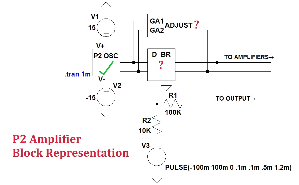
Figure 15. Simplified block representation showing how the oscillator, diode bridge, P2 inputs and gain/phase adjust interact.
By doing this, DC-related noise is significantly reduced (since information from the input signal is now “encoded” in AC).
To get a better feel of the diode bridge, I have prepared a test setup below.

Figure 16. The internal schematic of the P2 diode bridge.
The inductors provide DC isolation, with a coupling coefficient of 1. Diodes D1, D2, D3, and D4 are identical, modelled with a zero-bias junction capacitance of 105pF [default=0] and saturation current of 3pF [default=0.01 pA]. The signal entering OPAMPIN+ to OPAMPIN- will be superimposed on the signal entering OSCIN1 to OSCIN2. The output is at DBROUT1, with its 180° phase shifted version at DBROUT2.
Coupling 5MHz and 1 kHz sinusoids with the Diode Bridge.

Figure 17. Diode bridge test schematic for Case 1.
First, I test what will happen when I feed a 1 kHz and a 5 MHz sinusoid to the diode bridge block of the P2. Signal source/generator SS1 will supply the 1V pk-pk 1kHz sine wave while SS2 will provide a 5MHz signal of equal amplitude. I am theoretically expecting a signal with pronounced frequency components at 5MHz+1kHz and 5MHz-1kHz. Simulating yields the VOUT1 waveform below.

Figure 18. Simulation result of VOUT1 for test schematic in Figure 3.
Using the FFT to observe the frequency spectrum of VOUT1 yields the figure below.

Figure 19. FFT of VOUT1

Figure 20. Zoom-in view on the peaks of the FFT curve in Figure 5.
From the FFT plot, it is clear that the peaks are at 4.999 MHz and 5.001 MHz, verifying our theoretical expectations. Furthermore, the information in VSIG1 is visible at the envelope of VOUT1. Can you see it?

Figure 21. Where is the information of VSIG1?
Now we have an AC signal with information “riding” on it. All we have to do is amplify, then demodulate it before the output. Right? Not yet, there is one more bit of housekeeping that needs meticulous attention, and that is the diodes we choose for the bridge.
What happens when the diodes are mismatched? Let’s find out! Below, I’ve declared a new diode model, V48, with its saturation current at 7pA and zero-bias junction capacitance at 205pF.

Figure 22. Modified schematic for the P2 Diode Bridge. D2 has been mismatched.

Figure 23. Simulation result of Figure 8.
Mamamia! What has happened to our output? Can you imagine, increasing the saturation current by just 4pA and the capacitance by 100pF having such an effect on the output? To ensure that choice of values wasn’t a factor, I matched all the diodes again using V48, re-simulated, and got the proper waveform. It certainly must have been a daunting task to manufacture the P2 with 4 diodes that had such stringent matching conditions.
This isn’t the only instance matching played a crucial role in design. I believe the same rule applies for Kelvin bridges, or any similar circuit configurations, the only difference being a more relaxed demand in accuracy. How about current mirrors, who have to have MOS pairs that are identical to each other or else the “mirrored” currents would have offsets?

Figure 24. Schematic for adjusting offset in the P2.
This block isn’t the only one controlling the gain of the oscillator. Remember the C40 capacitor encircled in red back in part 1? I think it is meant to provide feedback from the AC demodulator (which makes sense, how can you demodulate/decode something if you have no idea or information on the code or original content used?) This discussion however, is for a future article.
Looking closer at the resistor-capacitor network, C11 and C12 are most probably variable capacitors, while R1 and R2 are potentiometers. Terminals GA1 and GA2 connect back to the oscillator while GADJIN1 and GADJIN2 connect to the outputs of the diode bridge. From part 2, we recall the most interesting component of the oscillator, C6, where the value of capacitance and amplitude of oscillation share an inversely proportional relationship, valid from 25pF to 1µF, after which oscillation stops. Looking back at Figure 10, I believe it is safe to assume that the capacitance will only vary in the pF range because series-parallel connections will cancel each other out. We should be surprised if we saw a capacitor here with a value of 1µF or more.
To conclude, let us simulate the schematic in Figure 1.

Figure 25. Simulation result of Figure 1.
Node 2 is the output of the diode bridge (shunted to the offset adjustment block). Node 7 is the input pulse to the diode bridge. Different combinations of x and y yield different results (less than 1 of course). When x and y are at very low values, the peak-to-peak voltage of node 2 approaches that of node 7. I think the default values set in Figure 10 are just right to prevent overmodulation.
Can you see the information riding on node 2?
0 Comments